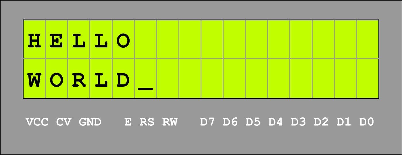
In this tutorial, we’ll interface the 8051 microcontroller with an LCD (Liquid Crystal Display) and display a blinking “Hello World” message.
Several months ago I knew nothing about electronics. Now I’m an electrical engineering major. Why? you might ask. If you’ve read any of my articles on Medium, you may know I’m a neuroscience and brain-computer interface enthusiast. While I headed into university thinking I’d study physics, I realized engineering would be more practical. Plus it’s super fun!
As I’m now delving into the world of computer engineering, I thought I’d take you along in a series of tutorials on programming the 8051 microcontroller using Assembly.
You can view my complete compilation of tutorials in this Github repository, and the code for this tutorial in this folder. Since I’m on break from university and don’t have access to the cool electronics from our lab, I’ll be using MultiSim to construct and program the microcontroller circuits. (You can download MultiSim on Windows with a free 7-day evaluation, extended to 45 days upon request.)
In this tutorial, we’ll interface the 8051 microcontroller with an LCD and display a blinking “Hello World” message. LCDs are widely used in electronics for displaying messages and data, so hopefully you can apply what you learn here to your other projects!
8051 microcontroller (MCU). Built with 40 pins, 4KB of ROM storage, 128 bytes of RAM storage, and 2 16-bit timers. It consists of four 8-bit input/output (I/O) ports, each with bidirectional ability, i.e., the ability to receive data as input or send data as output. We will use these ports to interface with the LCD, and primarily configure the ports to output data to the LCD.
LCD (Liquid Crystal Display). Electronic display module. Here we use a 16x2 LCD, which means there are two lines and each can display 16 characters. In this LCD, each character is displayed in a 5x7 pixel matrix.
Crystal. Generates clock pulses required for the synchronization of all internal operations. We connect it to pins XTAL1 and XTAL2 of the MCU. Here we use a frequency of 11MHz.
Capacitors C1 and C2. Serve as stabilizers, keeping the oscillator locked at the specified frequency. Here we set C1 = C2 = 33pF.
Bussed three-line resistor R1. Serves as pull-up resistor for port 0 pins (port 0 always requires external pull-up resistors). Here we use a resistance of 10K.
Now let’s dive a bit deeper and take a look inside the LCD to see what’s going on. Below is a block diagram of the 16x2 LCD, adapted from this source and the HD44780U (LCD-II) datasheet. It may be a bit overwhelming, but we’ll break it down.
Block diagram of 16x2 LCD, adapted from this source and the HD44780U (LCD-II) manual.
Let’s start with a high-level overview of the 16 pins of LCD module. When looking at a 16x2 LCD, you’ll see something similar to the figures below. The first is a representation of an LCD in MultiSim, and the second is an actual HD44780 LCD. You’ll only see 14 pins on the MultiSim representation since the backlight pins aren’t necessary.
Top: 16X2 LCD, as represented in MultiSim. Bottom: 16x2 LCD Display Module HD44780 Drive Yellow.
We can divide the pins into five categories: power, contrast, control, data, and backlight. A summary of the pins and their functions is shown in the table below. Don’t worry if you don’t understand what some of the functions mean yet.
The LCD has two 8-bit registers, namely the data and instruction registers.
Data register. Temporarily stores data to be written into or read from DDRAM or CGRAM.
Command register. Stores command codes, such as those to clear the display, set the cursor, and read/write data. Some common commands are shown below, where the codes are given by the values of RS, RW, and D0-D7.
There are three main memories in the LCD to manipulate character displays: DDRAM, CGROM, and CGRAM.
Display Data RAM (DDRAM). Stores display data represented in 8-bit character codes. Each address in DDRAM corresponds to a position on the LCD, shown in the figure below.
Character Generator ROM (CGROM). Stores all permanent character patterns, e.g., letters of the alphabet. It generates 5 × 7 dot (pixel) character patterns from the 8-bit character codes in DDRAM. (If you’re not using the cursor, it’s 5 x 8.) Note that the patterns are stored such that their memory address is equivalent to the ASCII code for that pattern.
The workflow for sending character ‘A,’ for example, would be as follows:
Character Generator RAM (CGRAM). Stores custom characters loaded by the user, e.g., a smiley face. This memory can store up to 8 user-defined characters, but as it is read-write memory, it is volatile and can be modified any time.
On the other hand, the workflow for loading a custom character would be as follows:
Step 1: Define custom character
Step 2: Display custom character
Notice the similarities between the last two steps of part two in this workflow with the last two in the standard character workflow, i.e., the one that uses CGROM.
Busy flag (BF). Checks the internal status of the LCD. When the busy flag is 1, the LCD is still executing previously-received commands and the next instruction will not be accepted. When the busy flag is 0, the LCD is ready to accept new information and the next instruction can be written.
Address counter. Assigns addresses to both DDRAM and CGRAM. Any time you write to DDRAM or CGRAM, the address counter automatically increments by 1. If you read from DDRAM or CGRAM, it decrements by 1.
Instruction decoder. Processes the command code written into the command register.
LCD driver. Receives low-level instructions and turns them into waveforms for controlling commons (COM) and segments (SEG), i.e., sub-units of the display. (For a good explanation of this, see this pdf).
Timing generation circuit. Generates clock signals to ensure the proper timing and thus operation of internal circuits such as DDRAM, CGROM and CGRAM.
Cursor/blink control circuit. Generates the cursor or character blinking. The cursor or blinking will appear with the character located at the DDRAM address set in the address counter.
Now that we have some background on the LCD structure, let’s discuss the control pins a bit more. Recall from the section on LCD pins that there are three signals that the microprocessor uses to control the data transfer with the LCD module. A summary of these pins and their functions is given in the table below.
RS (register select). As its name suggests, this pin switches between the command and data registers by setting RS = 0 or RS = 1, respectively.
RW (read/write). This pin switches between writing data to the LCD and reading data from the LCD by setting RW = 0 or RS = 1, respectively. (RW is usually set to 0 since only the “Get status” instruction requires it.)
E (enable). This pun functions as the command/data latching signal for the LCD. When E=0, the LCD does not care what is happening with RW, RS, and the data bus lines. When E = 1, the LCD is processing the incoming data. However, it is really an edge-triggered pin, in particular negative edge-triggered. This means the LCD will latch in whatever is on the Data Bits and process it on the falling edge of the E signal, i.e., transitioning from high (1) to low (0).
The diagram below shows the timing for the LCD write cycle, demonstrating the interactions between the RS, RW, E, and data (D0-D7) signals. All 8 data signals are grouped together in the bottom row as their individual values don’t matter in terms of influencing the events of the cycle.
At event 1, the RW signal is set low to indicate the LCD is ready to accept data, i.e., the MCU can write data. RS is set as high or low depending on whether the MCU is writing data or commands, respectively. The data signals are ignored during this period.
When the MCU has information to send to the LCD, it loads data to the Data Bits and then asserts the E signal high at event 2 to indicate the data is available to read.
At some point in the interval between events 2 and 4 (i.e., while E is high), the data byte is sent to the data lines and the LCD reads the data bus (event 3). The next region is labeled “valid data,” as this is the actual data that will be written to the LCD.
On the falling edge of the E signal at event 4, the LCD latches the data and the data is no longer available on the data bus. The data must not actually change until data hold time is met at event 5. The RS, RW, and data lines are all free to change to other values after event 5. The only thing that you can’t do is bring E high again too soon, as a certain time buffer is required between writes to the device.
The time intervals shown on the bottom of the diagram are all specified by the receiving device. To learn more about these, see the HD44780U datasheet.
Segments where signals are present in both high and low states indicate the state can take on either value. Image by author, inspired by the HD44780U datasheet.
If we put all that we’ve learned together about the LCD structure and programming the control pins, we end up with a diagram that looks as follows. (Note that this represents “write mode,” i.e., RW = 0, and only considers CGROM for simplicity.)
Path of data in LCD write cycle. Image by author.
Before we break down the code, we’ll go over Assembly implementation of three key concepts we’ll be using in our code:
We won’t be using “regular” while loops in our code, but if you’d like to see how they’re implemented in Assembly, see this article.
In Assembly, any sort of conditional jump instruction (e.g.,
JNC
, JNZ
, DJNZ
) can be used for implementing for loops, but most often we use DJNZ
(decrement and jump if not zero). In this directive, the register is decremented; if not zero, it jumps to the target address referred to by the label.The structure of a for loop in Assembly is shown in the code below. Prior to the start of the loop a register is loaded with the number of iterations you desire. Once we arrive at the end of the loop, we use the
DJNZ
directive, which combines the register decrement and the jump back to the beginning of the loop.An infinite loop is a sequence of instructions in a program that repeats endlessly.
To implement infinite loops, we now use the unconditional jump instructions,
SJMP
(short jump) and LJMP
(long jump). The difference between LJMP
and SJMP
is that LJMP
takes a two-byte absolute address, allowing you to jump to any memory location from 0000 to FFFF (hex), while SJMP
takes a one-byte relative address, allowing you jump to an address within a range of 00 to FF. Often, the target location we need to jump to is not that far, and since SJMP
takes one less byte of memory, it is our preferred choice.The structure of an infinite loop in Assembly is quite simple:
Similar to functions in high-level programming, subroutines are “self-contained” pieces of code in a program that accomplish specific sub-tasks. In a given program, we often need to perform a particular sub-task many times on different data values. Rather than repeat the same block of instructions every time, we can package the instructions in a subroutine to call upon when needed.
We can call a subroutine at any point in the program using the call instructions,
ACALL
and LCALL
. Similar to the situation with SJMP
and LJMP
, ACALL
restricts the target address to a smaller range than LJMP
but takes less memory.A subroutine is called by transferring control to its entry point, so when the subroutine completes its execution, it needs to return control back to the calling routine. Therefore, whenever we create a subroutine, we end it with a
RET
(return) instruction.An example of the structure of a subroutine and the routine that calls it is shown below.
Now, we’ll finally break down the code. Note that the order of this breakdown doesn’t align with the order of the code.
In assembly code, the
EQU
directive gives a symbolic name (label) to a numeric constant, a register-relative value or a PC-relative value. It is essentially the same as setting a variable in higher-level programming languages.Since we will use the RS, RW, and E pins a lot, we’ll assign symbolic names to the corresponding pins we’ve chosen (which depend on the wiring of the MCU to the LCD). In the circuit schematic above, you can see that bits 0, 1, and 2 of port 0 on the MCU have been wired to the RS, RW, and E pins, respectively.
We’ll also let
DATA_PORT
correspond to port 2, as bits 0–7 of port 2 are connected to pins D0-D7 of the LCD. We’ll discuss the labels defined in lines 6–7 in the section on the byte-looping subroutine.Let’s say that rather than using the symbolic names
RS
, RW
, and E
, we used P0.0
, P0.1
, and P0.2
everywhere. The first disadvantage of this is that if you changed the wiring such that the LCD control pins were connected to port 2 instead of port 0, you would have to replace every instance of P0 with P2. In the case of using variables, you would only have to change the defined ports and bits in the EQU
statements.The second disadvantage is readability. Looking through the code, you might forget, for example, that
P0.0
corresponds to RS. Using (well-named) variables eliminates this problem.In Assembly, the
DB
(define byte) directive defines a byte-size variable, which can be in decimal, binary, hex, or ASCII format. In the code below, hex format is indicated by appending an “H” to the numerical value, and ASCII format is indicated by placing characters in quotation marks. (The assembler will assign the ASCII code for the characters automatically.) DB
followed by multiple operands simply defines a succession of bytes. Note that if the operand is a string, it is already a succession of bytes, as each character takes one byte in memory.We can access the data we’ve defined by assigning labels before the directives. In other words, we create variables storing the data. Later, we’ll use these variables to load the data in the main program.
First, we define the variable
INIT_CMND
, which will hold a succession of commands to initialize the LCD display:38H
: 8-bit, 2 line, 5x7 dots0EH
: Display ON cursor, ON06H
: Auto increment mode, i.e., when we send char, cursor position moves rightThis, in effect, creates a lookup table at the
INIT_CMND
address. We can think of each command as an entry in a table, with 38H
being the first entry, 0EH
being the 2nd, and 06H
being the 3rd. The value of each entry can be accessed via its index in the table, which we will see come into play when we write both commands and data to the LCD one byte at a time.We define variables
LINE1
and LINE2
, containing the commands to bring the cursor to lines 1 and 2 in a similar fashion. Finally, we define variables DATA1
and DATA2
, containing the data to display on lines 1 and 2 of the LCD.Proper delays between actions in embedded systems are important so that the system has time to execute instructions. In our system, there are two ways we can ensure the LCD staggers its internal operations:
In practice, it is recommended to use the second method, as the delay produced is almost exactly the amount of time the LCD needs for processing. However, for our purposes, we’ll stick with the first method, which is simpler but serves the same purpose as long as the delay is appropriate. (For an example of method two, see this article.)
One classic way to make a delay is to use nested decrement loops. Every time the inner loop counts down to 0, then the next decrements, and so on. The code for the delay subroutine we’ll use is shown below.
We can calculate the length of the delay our subroutine produces by analyzing the number of machine cycles (MC) taken for each instruction and taking into account the number of repetitions. We’ll break down our calculations by the inner and outer loops.
MC of inner loop (L1)
MC of body: 2
Num repetitions: 4
Total MC: 4 x 2 = 8
MC of outer loop (L2)
MC of body: 1 + 8 + 2 = 11
Num repetitions: 255
Total MC: 255 x 11 = 2805
Not that it makes a big difference, but we can also add the MC of the first and last statements:
Total MC: 2805 + 3 = 2808
Now, we can find the delay in microseconds (us). The machine cycle for a system of 11.0592 MHz is 1.085 us, so the total delay of our delay subroutine is:
2808 x 1.085 us = 3.047 ms
From the LCD write cycle, recall the steps for sending a command:
The steps for sending data are similar, except RS is set high:
As you can see in the excerpts of code above, setting each pin low or high is relatively straightforward. The
CLR
directive is used for the former and the SETB
directive is used for the latter.Understanding the first step, loading the data port, was more difficult for me, so let’s dive a bit deeper. In both excerpts, lines 3–4 correspond to step 1. The values of A (the accumulator register) and the DPTR (data pointer) function as parameters passed to the subroutine, together addressing the desired byte of data or command in code space. Here’s how it works:
MOVC A, @A+DPTR
moves the (A+1)th table entry into A (we use MOVC
since the index is in code space).The GIF below shows a visual of this process. Here, DPTR points to
DATA1
and A iterates through each character of the data. (As a side note, a great way to debug your code is to check the values of registers at various “checkpoints.”)Iteration through lookup table using DPTR and A registers. Images by author.
So how do we control A in order to access all the entries in a table? That brings us to our next subroutine.
Since we write data and commands one byte at a time, we now define a subroutine that loops through each entry in a given lookup table (pointed to by DPTR) and sends it to the LCD.
Since Assembly is a low-level programming language, and thus cannot be object-oriented, we go about this using the following method:
WRT_DATA
or WRT_CMND
subroutine.Going back to the section on assigning symbolic names, you’ll see that we assign register 0 (R0) the symbolic name
NBYTES
, and use it for storing the number of bytes in a table of data or commands. We also assign register 1 (R1) the symbolic name BYTE_IDX
, and use it for tracking the current iteration we’re at when looping through the bytes.You’ll notice from the code excerpt below that we increment A indirectly via the value of
BYTE_IDX
. We do this because the WRT_DATA
and WRT_CMND
subroutines make use A for storing table entries, and simply incrementing A would make the index have a large offset.Now that we’ve defined all of our subroutines, we can create the main body of our program. We begin by initializing the LCD with the commands in the
INIT_CMND
table. We first point the DPTR to the table and then specify the number of bytes the table has — 3 since there are 3 commands. After these “parameters” are set, we can call the SEND_CMND_BYTES
subroutine.We then proceed to the main loop, which infinitely repeats itself.
As described for the initialization process, every time we prepare to send commands or data to the LCD, we point the DPTR to the appropriate table and specify the number of entries.
Congratulations, we made it to the end! We can finally put everything together. Remember to check out my Github for the program and MultiSim files, as well as other 8051 projects!
👋 I am Danielle Gruber and I am a freshman at Yale University. I am an electrical engineering major interested in neuroscience, computer science, math, and everything in-between.
Contact me 👇
Gmail: [email protected]