
337 reads
PCB Testing Methods Overview
by byAndrey Solovev@andreysolovev
Co-founder and CTO at Integra Sources. PhD in Physics and Mathematics.
February 4th, 2022


Co-founder and CTO at Integra Sources. PhD in Physics and Mathematics.


Co-founder and CTO at Integra Sources. PhD in Physics and Mathematics.
About Author
Co-founder and CTO at Integra Sources. PhD in Physics and Mathematics.
Comments
TOPICS


Related Stories


Halo Principle Explained

Aug 15, 2021
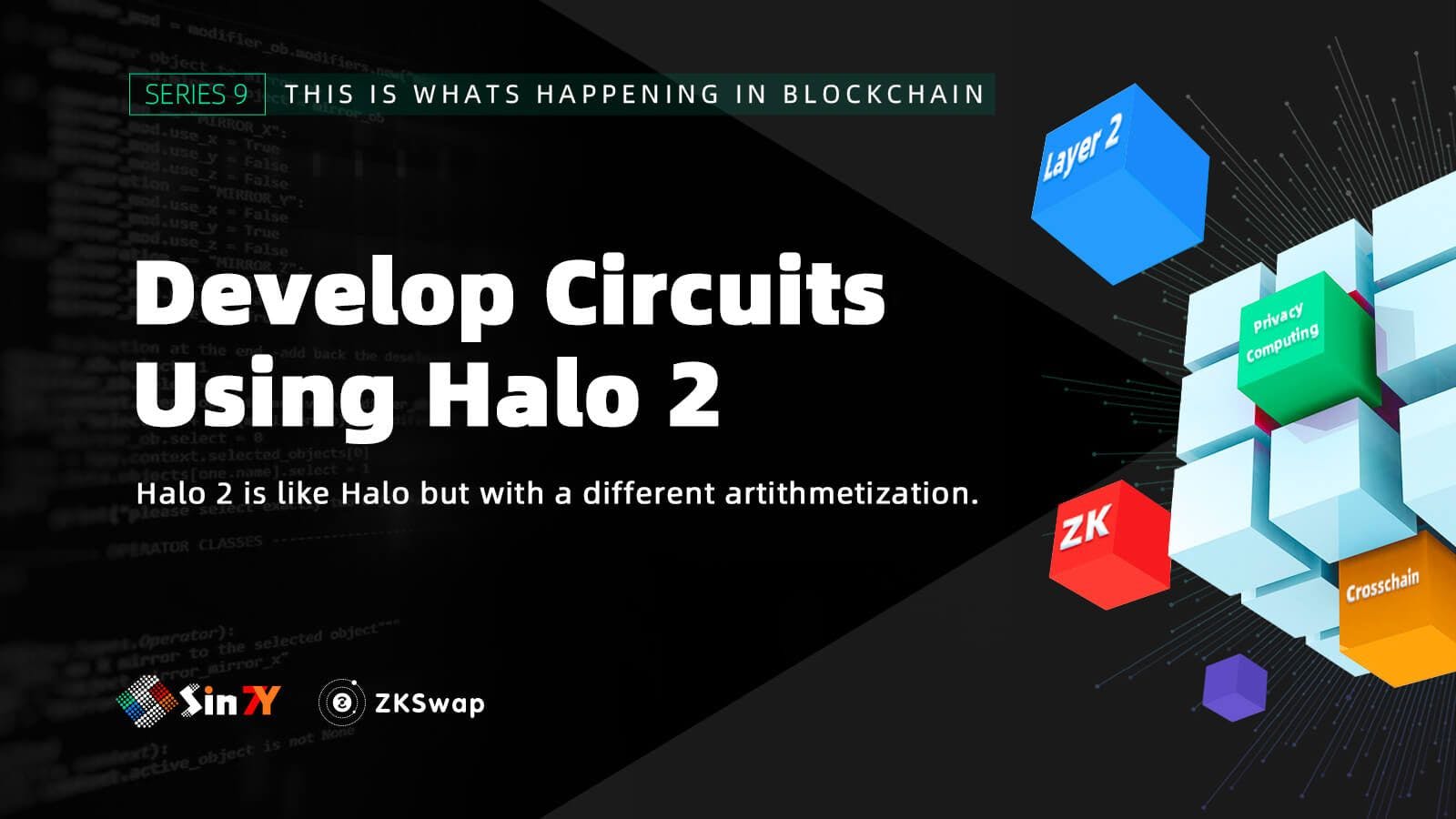
Halo Principle Explained
Aug 15, 2021